Technical documentation · Elyssa
Everything you need
to wire it up.
Do not guess, check. The schematic, the pinout, which pins are safe for what, and the power limits, straight from the board files and the open-source repository. Built to save you hours (and a few chips).
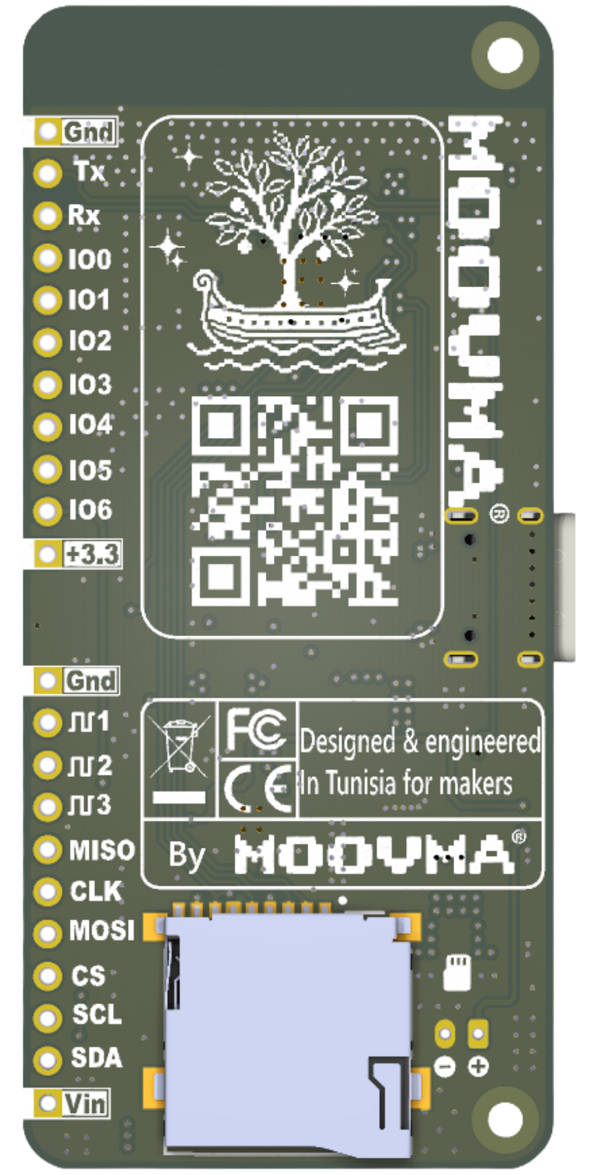
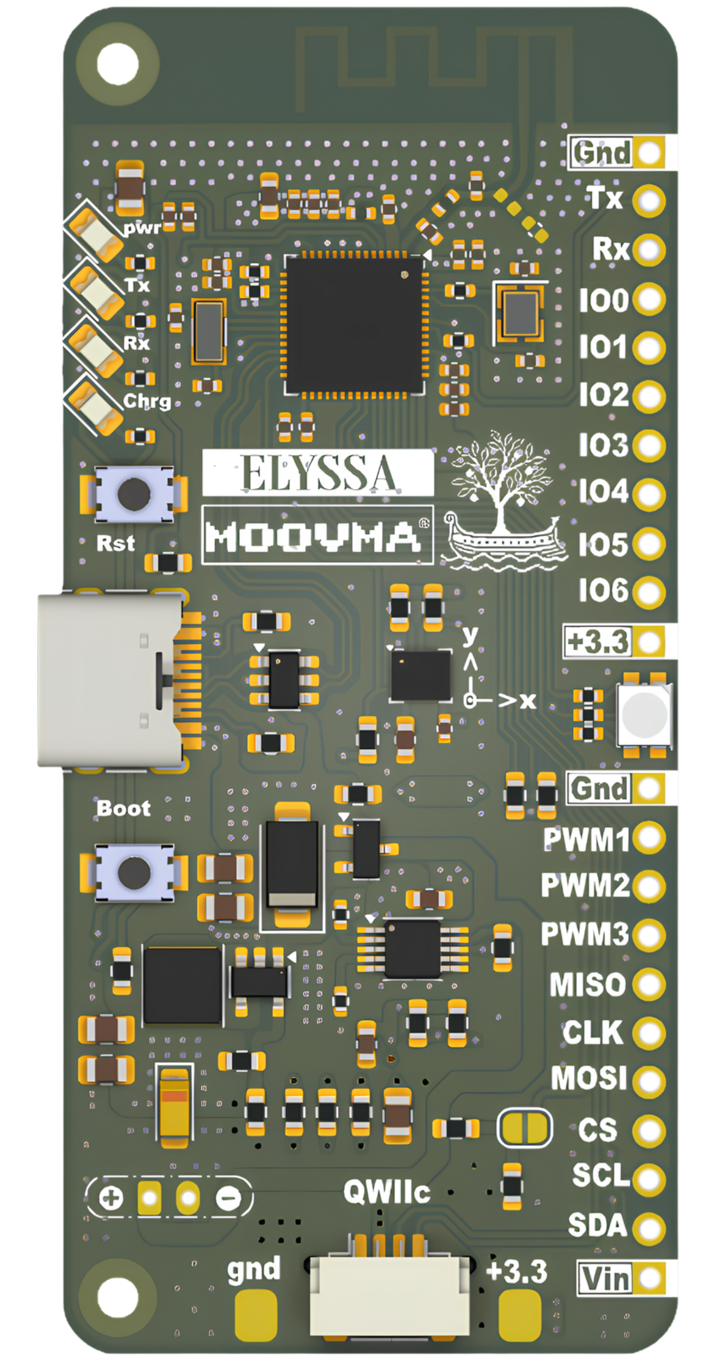
Header J12, top to bottom.
Names follow the silkscreen and work in sketches without any #include. IO0 to IO6 are GPIO1 to GPIO7. There is no A7 and no T7.
- 01Gnd—Ground
- 02TxGPIO43UART TX
- 03RxGPIO44UART RX
- 04IO0GPIO1A0 · T0 · digital
- 05IO1GPIO2A1 · T1 · digital
- 06IO2GPIO3A2 · T2 · digital
- 07IO3GPIO4A3 · T3 · digital
- 08IO4GPIO5A4 · T4 · digital
- 09IO5GPIO6A5 · T5 · digital
- 10IO6GPIO7A6 · T6 · BAT_SENSE (JP3)
- 11+3.3—3.3 V rail
- 12Gnd—Ground
- 13PWM1GPIO14PWM · or touch T10
- 14PWM2GPIO47PWM
- 15PWM3GPIO48PWM
- 16MISOGPIO37SPI MISO
- 17CLKGPIO36SPI SCK
- 18MOSIGPIO35SPI MOSI
- 19CSGPIO34SPI SS
- 20SCLGPIO9I2C SCL · A9 · T9
- 21SDAGPIO8I2C SDA · A8 · T8
- 22Vin—5 V, wired to USB (see the power rules)
- Power / ground
- Analog · touch · digital
- UART · SPI · I2C
- PWM
Is this pin safe?
Type the name printed next to a pin to see what it does and whether it is safe to use. Want everything at once? Open the full table.
Type a pin, or tap one of the examples, to see everything about it.
Power, regulation and limits.
Four rules to read before you plug anything in, then every number that matters.
- 01One power source on VinThe USB line is wired to the Vin pin. Never connect USB and an external supply to Vin at the same time: it can backfeed and damage your setup or your computer.
- 023.3 V logic onlyEvery GPIO works at 3.3 V and is not 5 V tolerant. Use a level shifter for 5 V signals.
- 03Go easy on the pinsKeep each GPIO under about 20 mA. For motors, relays and strips of LEDs, switch them with a transistor or driver.
- 04Single-cell batteries onlyThe charger is made for one 3.7 V Li-Ion or Li-Po cell, charged to 4.2 V. Never connect two cells or any other battery type.
| Item | Value | Notes |
|---|---|---|
| Main 3.3 V rail | Up to 2 A | A TLV62569DBVR step-down (buck) regulator with a 2.2 µH inductor drives the 3.3 V rail: efficient, steady, and plenty of headroom for sensors and modules. |
| USB-C input | 5 V | Programming, serial monitor and power over one cable. Use a data cable. |
| Vin pin | 5 V, wired to USB | Take 5 V out of this pin, or power the board from it when USB is unplugged. Never feed Vin while USB is connected. |
| Input protection | PMOS + Schottky diode | A power-OR stage protects the input and stops current flowing back between power sources. |
| LiPo charger | BQ24092 · about 540 mA | Charges one cell from the 5 V USB input. The 1 kΩ ISET resistor sets the current. There is no GPIO for it: the CHG output only drives the red charge LED. |
| Battery | 1S Li-Ion / Li-Po, 3.7 V | Charged to 4.2 V. A 1500 to 2000 mAh cell is a good balance between charging time and battery stress. |
| Charger temperature | Warm, up to about 125 °C | The charger chip can get noticeably warm. Around 125 °C its thermal regulation lowers the charging current automatically. |
| Battery voltage reading | VBAT / 2 on IO6 (GPIO7) | Only after bridging solder jumper JP3. In a sketch: vbat = analogReadMilliVolts(BAT_SENSE) × 2 / 1000. |
| Logic level | 3.3 V | GPIOs are not 5 V tolerant. |
| Current per GPIO | Under 20 mA | Use a transistor or driver for anything heavier. |
| Analog inputs | 0 – 3.3 V, 12-bit (0 – 4095) | ADC1 pins (IO0 to IO6, SDA, SCL) work with Wi-Fi on. PWM1 is on ADC2, which cannot be used while Wi-Fi is on. Use analogReadMilliVolts() for a calibrated reading. |
| RGB LED | 330 Ω per channel | Green looks brighter than red and blue. Balance mixed colours with setLedRGB(). |
| I2C | 4.7 kΩ pull-ups to 3.3 V | The header and Qwiic share GPIO8 / GPIO9. The IMU runs on its own bus at 400 kHz. |
| Wi-Fi transmit power | 11 dBm by default | Set by the board package for a reliable link. Above 12 dBm the connection can fail or slow down. |
| Bluetooth LE | −12 to +20 dBm | Advertising power range available on Elyssa. |
Elyssa is an open-source development board, provided “as is”. Moovma is not responsible for any damage, loss or malfunction caused by using it, by connecting it incorrectly, or by going beyond the limits on this page. Always double-check your wiring and power before you plug anything in.
Still have a question?
Ask about pins, power or the pre-order. Send the form and we reply by email, or write to moovmabh@gmail.com.
Pre-order Elyssa